
Semiconductor name typing — 8 lithography equipment names
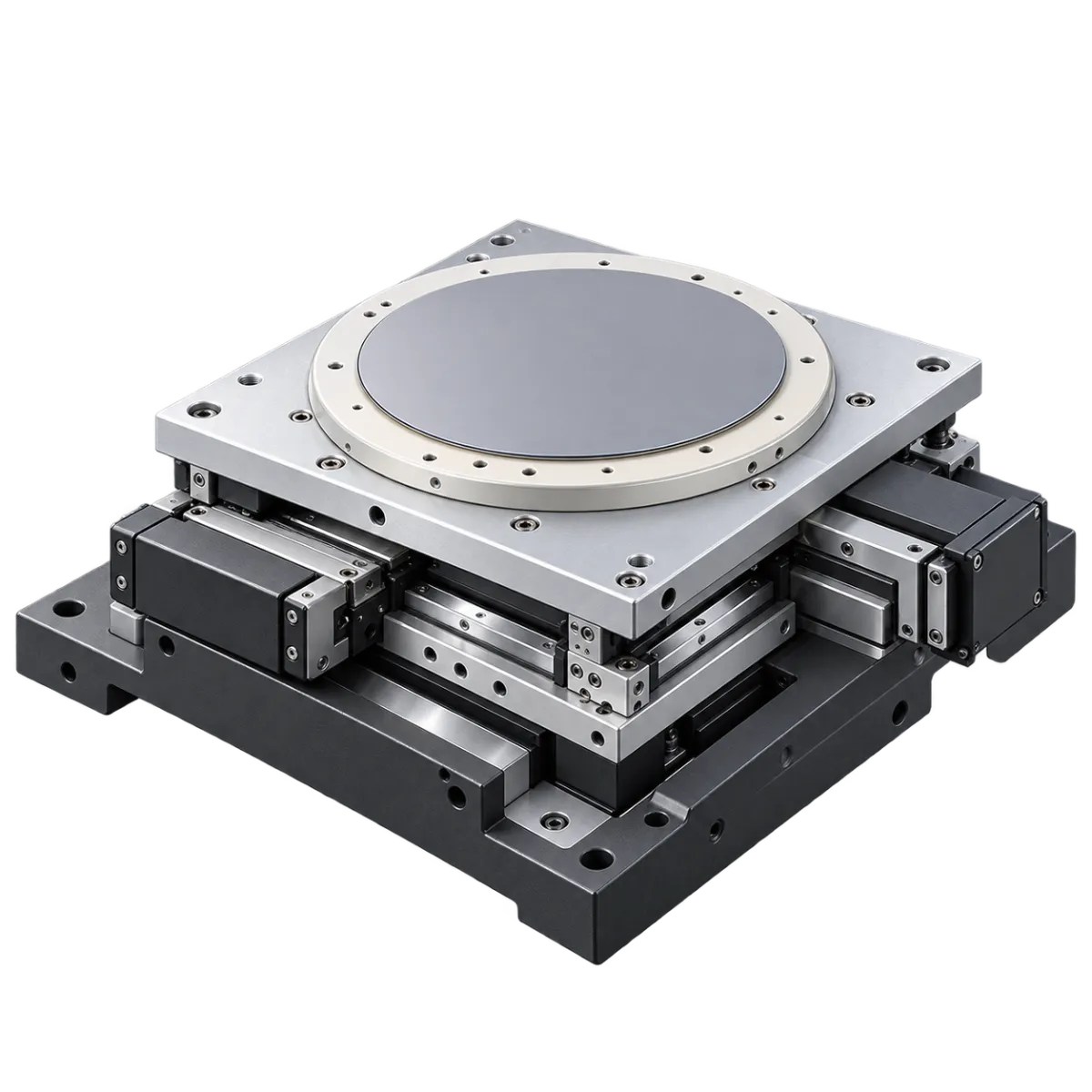
Wafer stage
Type the displayed name or a registered alternative to advance automatically.
You typed every name
Set complete!
New best time!
8 lithography equipment names name list
- Wafer stage
- Reticle stage
- Wafer handler
- Reticle handler
- Projection lens assembly
- Projection mirror assembly
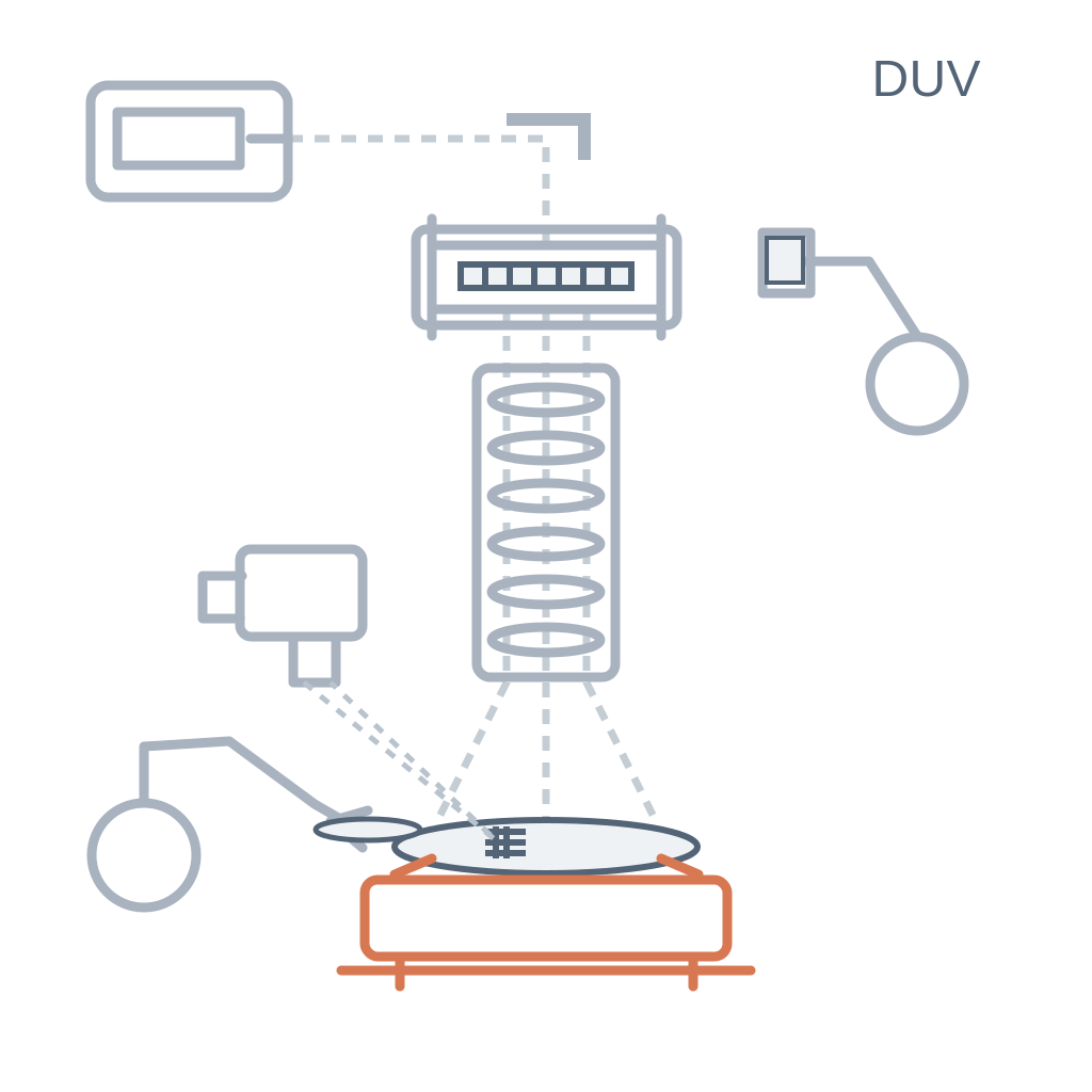
- DUV light-source module
- Wafer alignment sensor
Type 8 names in the 8 lithography equipment names set, from Wafer stage to Wafer alignment sensor. Read wafer and reticle separately, then distinguish a stage from a handler. Device pictures are symbols, not physical packages. Equipment pictures and placement diagrams are generic models for understanding function. They do not reproduce a commercial machine design or an optical prescription. A partition or relationship in a model should not be read as an exact engineering arrangement. Focus on the names and on the different purposes of the two illustration types.
Devices use circuit symbols; equipment uses generic educational models. Placement diagrams do not reproduce commercial designs or optical prescriptions.
Image sources and licenses
Circuit symbols: KiCad Library Contributors. This project converted them to SVG, standardized scale and line colors, omitted values and reference numbers, and added terminal labels and auxiliary function diagrams. All symbol SVGs are CC BY-SA 4.0. Separately generated equipment illustrations and placement diagrams are excluded from that license.